Multi-Project Wafer (MPW) Service


CORNERSTONE provides highly accessible Multi-Project Wafer (MPW) services for silicon photonics, enabling cost-effective access to advanced prototyping and small-volume fabrication.
MPW runs allow multiple designs from different users to be fabricated on a shared wafer, significantly reducing the costs and risks of photonic chip development. This model is ideal for:
- Early-stage industrial R&D
- Academic institutions
- Start-ups and SMEs
- Proof-of-concept prototyping
Why Choose MPW?
Cost-Effective Access:
Share wafer area and process costs with other participants, making advanced fabrication more affordable.
Accelerated Development:
MPW runs are scheduled regularly, helping teams reduce time to test and iterate on photonic designs.
CMOS-Compatible Processes:
Our platforms use industrial-grade lithography, ensuring seamless scalability from prototype to volume.
Flexible Design Entry:
From standard component libraries to process design kits (PDKs), our design enablement infrastructure supports a broad range of experience levels.
Community-Driven Innovation:
CORNERSTONE’s open-access model and advisory board ensure the platform evolves in line with user needs, fostering collaboration across academia and industry.
C‑PIC Member Discount:
Eligible organisations enjoy 50% off MPW participation as part of the CORNERSTONE Photonics Innovation Centre (C‑PIC) community.
Whether you’re developing components for telecommunications, quantum technologies, sensing, or integrated photonics research, our MPW service offers a streamlined path from concept to physical chip.
MPW Process:
From Design to Fabricated Chip
CORNERSTONE’s MPW service offers a simplified process for the design and fabrication of chips, accelerating your Silicon Photonics project through these straightforward steps:

Step 1: Review MPW Schedule & Costs
CORNERSTONE offers a range of silicon photonics platforms—including SOI, Ge-on-Si, and SiN—suitable for applications in telecommunications, sensing, LiDAR, quantum, and more. MPW runs are scheduled regularly, each tied to a specific technology platform.
To plan your submission:
- View our MPW Schedule & Costs page for upcoming run dates, platform details, and pricing.
- Identify the MPW run that aligns with your development goals and timeline.
![]()
Step 2: Sign Up for the Next Compatible MPW
When you have chosen your MPW call:
- Complete the MPW Sign-Up Form, providing details about your project and organisation, before the stated deadline.
- Our team will confirm your submission and issue a quotation.
- In the meantime, you can start the process of generating a purchase order. If you need to set us up as a supplier, please contact us.

Step 3: Prepare Your Design
Designs can be created using your own tools or with support from our PDKs and standard component libraries.
To ensure your design is compatible:
- Download the relevant Design Guidelines for your chosen platform.
- Use our GDSII templates to structure your layout.
- Refer to the Standard Components library for pre-designed photonic elements.
- Run checks using the Design Rule Check (DRC) checklist.
All resources are available on our Live MPW Calls pages.
![]()
Step 4: Submit your MPW design
Once your design is ready:
- Upload your design file using the provided submission form before the stated deadline.
- You will be required to upload a Purchase Order (PO) to this form to complete your submission.

Step 5: Design rule checks
Our team will perform design rule checks on your submitted design.
- You will be given the opportunity to correct any design rule violations.
- Resubmit your corrected design by the stated design acceptance deadline
All resources are available on our Live MPW Calls pages.

Step 6: Fabrication Process
Following the submission deadline:
- Your design is integrated into the MPW run.
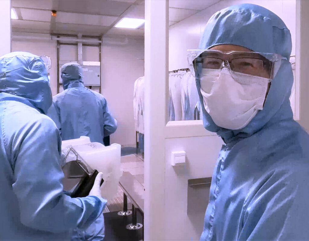
- Fabrication is performed by our team.
- Comprehensive quality assurance, including optical and physical metrology, ensures fabrication consistency.
After fabrication is completed:
- Your fabricated dies will be delivered as per the agreed schedule.
- Additional post-processing or packaging services can be arranged upon request.
Ready to Start?
If you require any assistance with design, platform selection, or schedule planning, please contact the CORNERSTONE team directly.

Bespoke Fabrication runs
If you have an exciting idea you’d like to discuss before signing up, please get in touch.
We love hearing about new research directions and can offer:
- Design consultancy
- Bespoke fabrication packages
- Support to help bring your concept to life

EUROPRACTICE
CORNERSTONE is accessible via EUROPRACTICE, a consortium of research organisations that provides European industry and academia with a platform to develop electronic and photonic circuits and systems.
Find out more about Europractice
JePPIX
CORNERSTONE is accessible via JePPIX, the European platform that brings together the InP and Triplex PIC supply chain through an open-access foundry model, supporting industry and academia in developing photonic integrated circuits.
Find out more about JePPIX