Technology Platforms
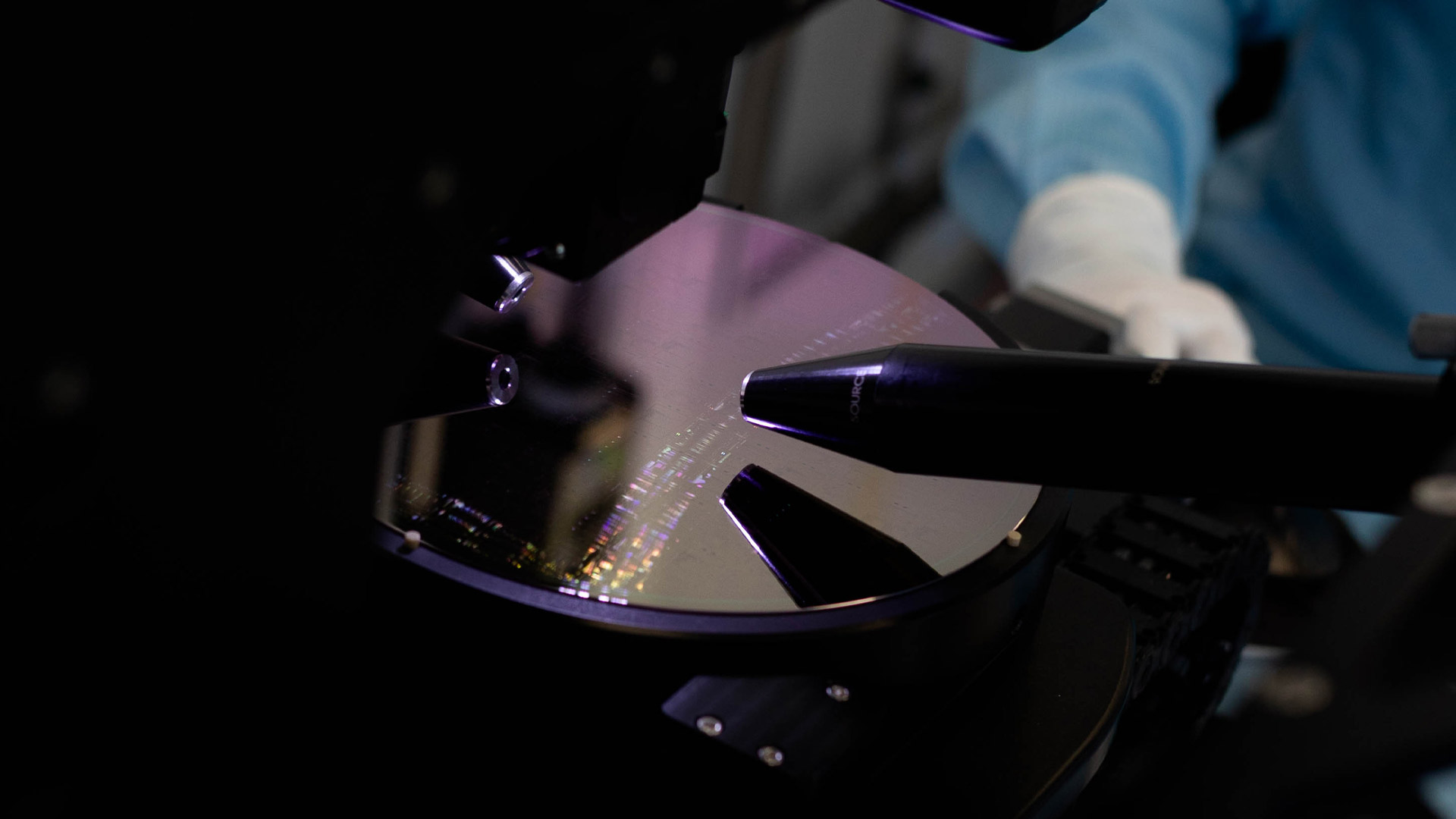
We offer a variety of platforms to suit your applications
With wavelength coverage spanning from the visible spectrum to the mid-infrared, our platforms enable an exceptional range of applications from high-speed datacom to quantum technologies, biosensing, and beyond.
If you require any assistance with design, platform selection, or schedule planning, please contact the CORNERSTONE team directly.
220 nm silicon-on-insulator (passive devices / active devices)
Our team has an exemplary track record in silicon-based modulators having demonstrated several world firsts, including the first 1 Gb/s carrier depletion modulator in 2004, now the industry standard, and the first 50 Gb/s carrier depletion modulator in 2012. In 2020, we demonstrated a fully integrated silicon MZI modulator with CMOS driver operating at 100 Gb/s OOK. More recently in 2025 we demonstrated 200 Gb/s OOK.
| Technology details |
Si etch depths: 70 nm, 120 nm & 220 nm TiN based thermal phase shifters 4 implantation layers for active device batches High resistivity handle wafer for improved RF performance (750 ohm.cm) |
| Performance (TE single mode @ λ = 1.55 µm): | Rib waveguide propagation loss: < 3 dB/cm Strip waveguide propagation loss: < 4 dB/cm Grating coupler loss: 5-6 dB/grating Phase shifter efficiency (MZI): < 20 mW/π Modulator performance (1.8 mm long MZI based carrier depletion):
|
| Logistics | Design area options: 11.47 x 4.9 mm² / 5.5 x 4.9 mm² Delivery timeframe and cost: Refer to schedule and cost page. |
340 nm silicon-on-insulator (passive devices)
Our flexibility enables users to add customised steps into all of our MPW batches. For example, in this platform a user could add e-beam written apodised grating couplers capable of coupling efficiencies of < 1 dB. A user could also add customised etch depths or sensing windows in the top cladding layer.
| Technology details |
Si etch depths: 140 nm & 340 nm TiN based thermal phase shifters |
| Performance (TE single mode @ λ = 1.55 µm): | Rib waveguide propagation loss: < 2 dB/cm Strip waveguide propagation loss: < 4 dB/cm Grating coupler loss: 5-6 dB/grating Phase shifter efficiency (MZI): < 20 mW/π |
| Logistics | Design area options: 11.47 x 4.9 mm² / 5.5 x 4.9 mm² Delivery timeframe: < 3 months |
500 nm silicon-on-insulator (passive devices)
All of our platforms are supported by an open source process design kit (PDK), which is available to download in GDSII format or is accessible via our software partners.
| Technology details |
Si etch depths: 160 nm & 300 nm TiN based thermal phase shifters |
| Performance (TE single mode @ λ = 1.55 µm): | Rib waveguide propagation loss: < 3 dB/cm Grating coupler loss: 5-6 dB/grating Phase shifter efficiency (MZI): < 20 mW/π |
| Logistics | Design area options: 11.47 x 4.9 mm² / 5.5 x 4.9 mm² Delivery timeframe: < 3 months |
300nm silicon nitride
The SiN platform enables low-lost passive circuits and also opens up the possibility of supporting high optical power applications. The lower refractive index of SiN, relative to Si, also makes it less susceptible to fabrication tolerances and temperature fluctuations.
| Technology details |
Platform: 300 nm SiN / 3 μm BOX SiN etch depth: 300 nm |
| Performance (TE single mode @ λ = 1.55 µm): | Strip waveguide propagation loss: < 0.5 dB/cm Grating coupler loss: < 10 dB/grating |
| Logistics | Design area: 11.47 x 15.45 mm² Delivery timeframe: < 3 months |
Visible silicon nitride
The visible SiN platform extends the available operating wavelengths of CORNERSTONE’s portfolio into the visible range. This is of particular interest for quantum photonics technologies and biosensing. Both of our silicon nitride platform offer a top cladding opening step to expose the silicon nitride waveguides.
| Technology details |
Platform: 200 nm SiN / 3 μm BOX SiN etch depth: 200 nm |
| Performance (TE single mode): | Strip waveguide propagation loss: Depends on wavelength Grating coupler loss: Depends on wavelength |
| Logistics | Design area: 11.47 x 15.45 mm² Delivery timeframe: < 3 months |
Suspended-silicon
The SOI BOX layer becomes highly absorbing at wavelengths above ~3.8 μm. CORNERSTONE’s suspended-Si platform alleviates this problem by locally removing the BOX layer underneath suspended waveguides to extend the transparency of the SOI platform up to ~8 μm.
| Technology details |
Platform: 500 nm Si / 3 μm BOX Si etch depth: 500 nm, followed by HF etching for undercutting / suspension |
| Performance (TE single mode): | Waveguide propagation loss: < 1 dB/cm @ λ = 3.8 μm < 3 dB/cm @ λ = 7.7 μm |
| Logistics | Design area options: 11.47 x 4.9 mm² / 5.5 x 4.9 mm² Delivery timeframe: < 2 months |
Germanium-on-silicon
The Ge-on-Si platform supports wavelengths up to ~14 μm, which makes it well suited for a broad variety of applications including environmental, biological, chemical and pharmaceutical sensing, industrial process control, toxin and contaminant detection, point-of care diagnostics and astrophysics.
| Technology details |
Platform: 3 μm Ge-on-Si (n-type) Ge etch depth: 1.8 μm Edge couplers formed by custom dicing process |
| Performance (TE single mode): | Waveguide propagation loss: < 1 dB/cm @ λ = 3.8 μm < 1.5 dB/cm @ λ = 6.1 μm < 3 dB/cm @ λ = 7.6 μm |
| Logistics | Design area: 11.47 x 15.45 mm² Delivery timeframe: < 2 months |
Stay in touch
We’d love to send you our newsletter. You’ll be the first to hear about the latest MPW runs, training opportunities and news.
Join Mailing List