Completion: In progress

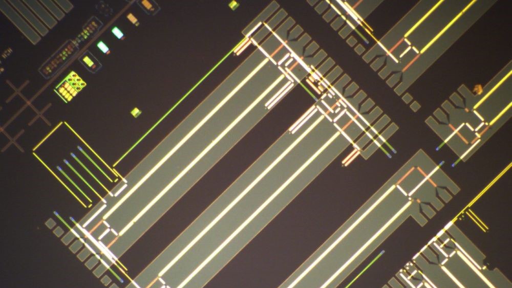
SOI 220 nm active and passive platforms
The platform features a 220 nm thick silicon device layer on a 2 µm buried oxide layer and is accessible through MPW and bespoke fabrication runs. Available in both active (with dopant implantation) and passive (with integrated heaters) runs, it enables the design of high-speed modulators. Our team has an exceptional track record in silicon-based…
Process Design Kit (PDK) TEST

Bespoke Fabrication Enquiry Form
Please enable JavaScript in your browser to complete this form.Name *FirstLastEmail *Telephone numberCompany/organisation *Shipping address *Which technology platform are you interested in? *SOI 220 nm ActiveSOI 220 nm PassiveSOI 340 nmSOI 500 nmSiN 300 nmSiN 200 nm VisibleGe-on-SiSuspended-SiOtherNote: all our processes are on 8 inch wafersWhat is the smallest feature size in [nm] you require?…
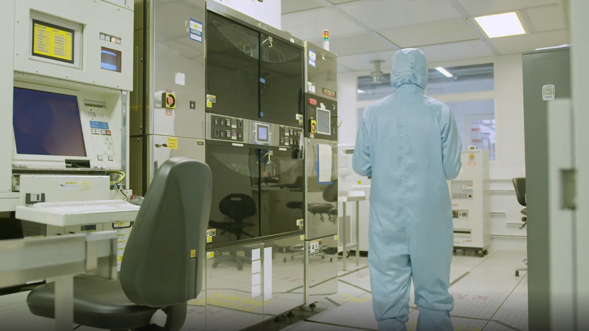
Multi-project-wafer (MPW)

MPW Schedule & Costs
MPW Schedule