Wafer-Scale Testing Service (WST)
Full 8” wafer optical yield mapping before dicing – propagation loss · insertion loss · C-band
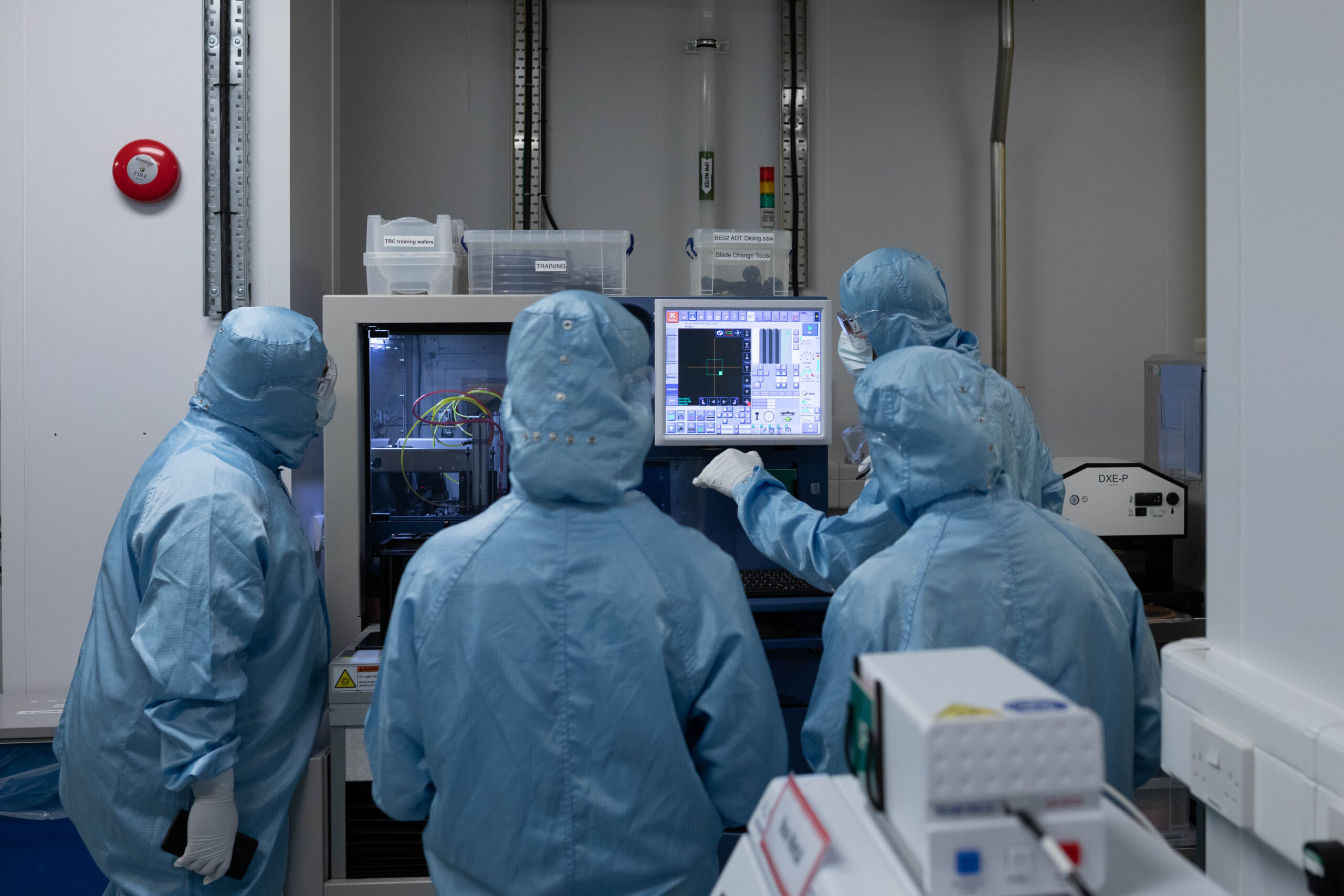
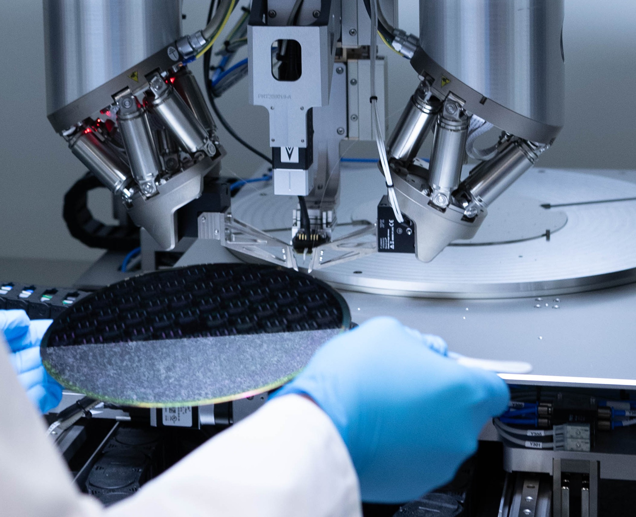
A single die measurement tells you what one device achieved. A wafer map tells you what your process delivers – across your wafer, every run. Our automated wafer-scale service measures optical performance across an 8” wafer in a single uninterrupted run, giving foundry teams and device developers the spatially-resolved yield data they need before any downstream commitment is made.
What sets this service apart
- Full wafer coverage in a single automated run: Dies across the 8” wafer tested to the same calibrated standard.
- Pre-dicing decision point: Optical performance data before the wafer is diced and before packaging costs are incurred – yield failures identified at the earliest possible stage.
- Wafer maps, not just device values: Spatially-resolved maps of propagation loss and insertion loss across the full wafer – uniformity and run-to-run consistency that single-die measurements cannot reveal.
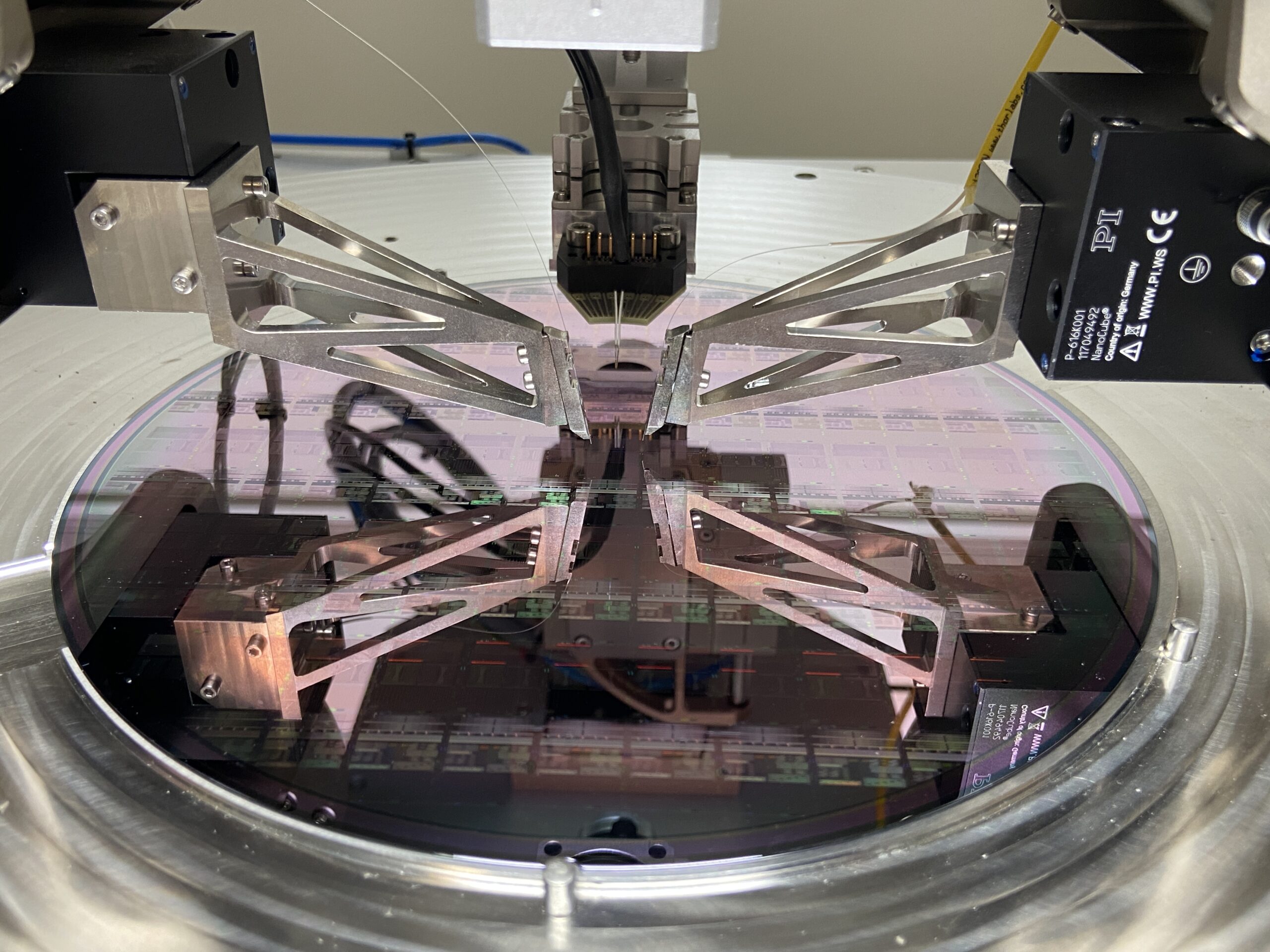
- ficonTEC platform: Built on the ficonTEC system – trusted by leading photonic foundries for automated wafer-scale testing – with precise automated fibre-to-chip alignment across the full 8” wafer area.
Measurement capabilities
Propagation loss mapping
- Waveguide propagation loss measured at different locations across the full 8” wafer
- Cutback test structure methodology – loss extracted per measurement site and aggregated into a full wafer map
- Strip and rib waveguide geometries supported
- Results reported in dB/cm
Insertion loss mapping
- Fibre-to-chip coupling efficiency characterised across the wafer
- On-chip component insertion loss: splitters, MMI structures, directional couplers, and other passive elements
- Results mapped across the wafer to reveal spatial trends and identify process-induced outliers
Measurement conditions
- Tunable laser source covering the C-band (1520 – 1630 nm)
- Automated fibre alignment to grating couplers
- All measurements performed on unpackaged, undiced 8” wafers
Who this is for
Whether you are a foundry team monitoring process yield, a device developer seeking performance data before committing to dicing and packaging, or a research group characterising a new photonic platform at scale, our wafer-scale test service provides the throughput and statistical coverage you need to make informed decisions with confidence.
- Foundry process monitoring and run-to-run yield tracking
- Pre-dicing yield assessment before packaging investment is committed
- Within-wafer uniformity characterisation for process optimisation
- New photonic platform development requiring statistically significant device data