
Chip-Level Testing Service
Passive and active device characterisation – directly on chip, across the full telecom window.
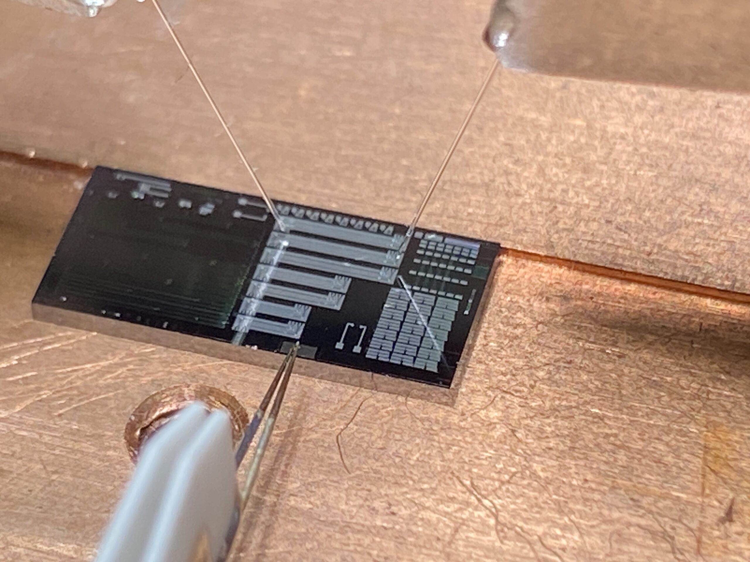
Chips back from the fab? Before packaging, shipment, or the next design iteration, you need to know exactly how they perform. Our chip-level testing service covers the full picture – optical loss, modulator behaviour, heater efficiency, bandwidth, and temperature dependence – all measured directly on the chip, without packaging.
What sets this service apart
- Passive and active – one service: From waveguide loss and coupling efficiency to modulator transfer functions and heater performance, the full picture in a single request.
- No packaging needed: We probe directly on the chip – characterise early, before packaging decisions are made, with no packaging-induced uncertainty in the results.
- Heater modulation bandwidth up to 160 MHz: Dynamic response of thermal phase-shifters measured across frequency – drive-voltage dependent upper limit.
- Reliable, calibrated results: Every measurement is made on calibrated, industry-standard equipment. Accurate and reproducible data you can act on with confidence.
Measurement capabilities
Insertion loss and spectral response
- Fibre-to-chip coupling loss characterisation for grating coupler and edge coupler interfaces
- On-chip component insertion loss: splitters, directional couplers, MMI structures, bends, and tapers
- Wavelength-swept transmission across O-band (1260 – 1360 nm) and C-band (1520 – 1630 nm) supported
- TE and TM polarisation-resolved measurements via in-line fibre polarisation controller
Propagation loss
- Waveguide propagation loss using the cutback method or ring resonator linewidth fitting
- Strip and rib waveguide geometries supported
- Loss reported in dB/cm
Thermal phase-shifter (heater) characterisation
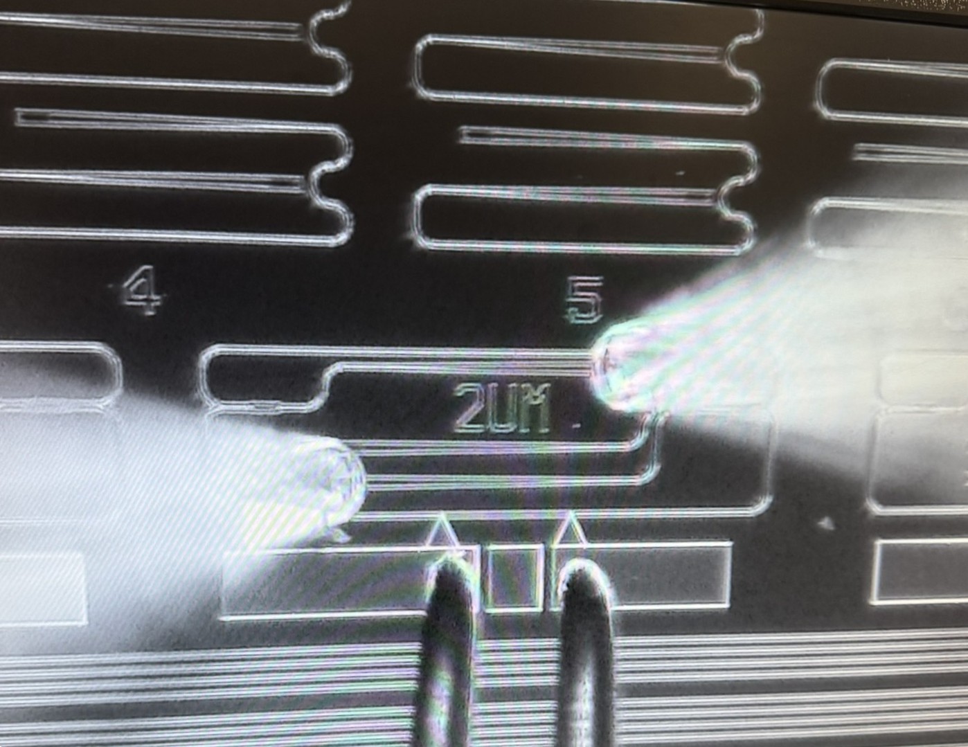
- Half-wave power (Pπ) for a π phase shift
- Tuning efficiency in pm/mW
- Thermal tuning range and linearity
- Thermal crosstalk between adjacent heater elements
- Heater modulation bandwidth up to 160 MHz – upper frequency limit decreases with drive voltage
Temperature-dependent characterisation
- Device performance measured across a defined temperature range using a calibrated temperature-controlled chip holder
- Applicable to insertion loss, propagation loss, modulator transfer function, and phase-shifter tuning efficiency
- Enables device qualification against real operating temperature conditions
PN-junction modulator characterisation
- Transfer function: transmission versus DC bias voltage
- Half-wave voltage (Vπ) at quadrature
- Modulation efficiency (Vπ·L) in V·cm
- Phase shift linearity with applied voltage
- Free spectral range (FSR), extinction ratio (ER), and effective refractive index
- Optical insertion loss at quadrature bias
- Results normalised against on-chip reference waveguides
- Ring resonator modulators: resonance shift vs bias voltage, Q factor, and effective index change also characterised where applicable
Need bandwidth measurements above 160 MHz? If your chip contains a high-speed modulator or photodetector and you need characterisation in the 10 MHz – 110 GHz range, see our High-Speed Testing (LCA) service.
Custom test support
- Diced chip configurations supported
- Compatible with multiple photonic platforms – SOI, SiN, Ge-on-Si, and suspended silicon – across visible and telecom wavelengths
- Integration with customer-supplied equipment where required