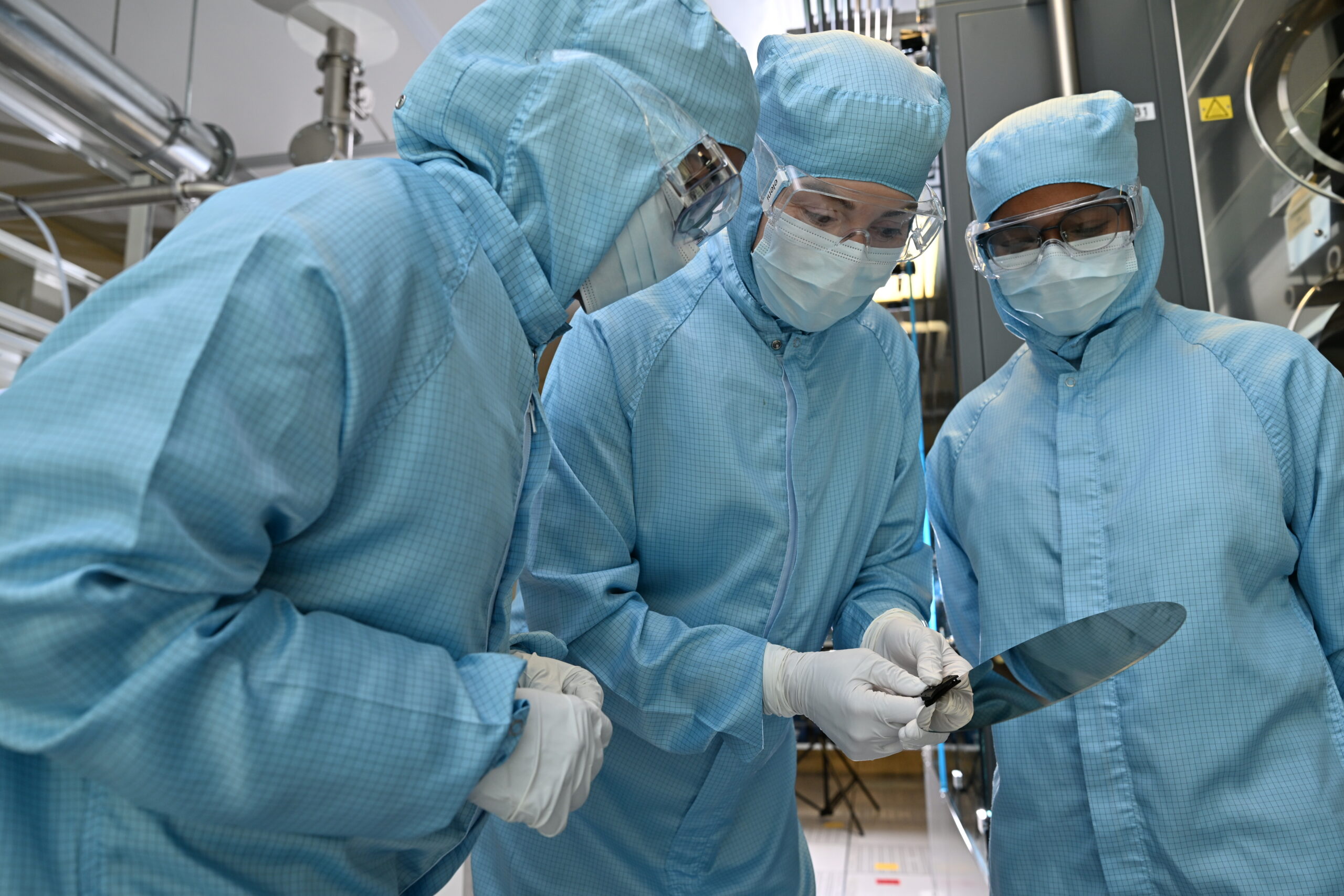
Lightwave Component Analyser (LCA)
The UK’s highest-bandwidth open-access electro-optical vector characterisation service – 10 MHz to 110 GHz
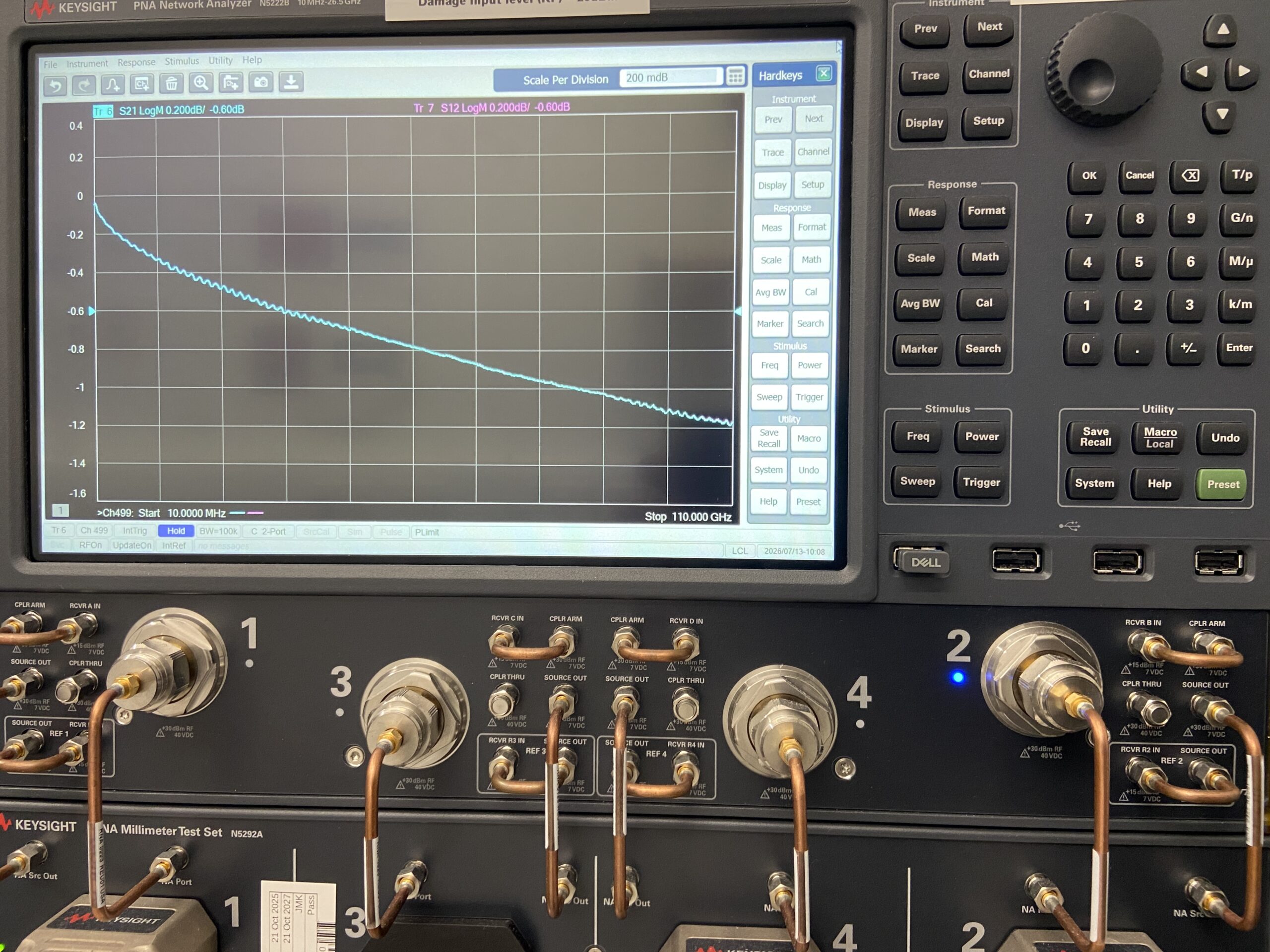
High-speed photonic device design is only as good as the data behind it. A bandwidth figure tells you where the response falls off – it does not tell you why or give you the complex transfer function your device models and system simulations actually need. CORNERSTONE’s LCA service closes that gap: full vector EO S-parameters – magnitude, phase, and group delay – from 10 MHz to 110 GHz, on bare die, across the full telecom window, with NIST-traceable calibration.
What sets this service apart
- Highest bandwidth in the UK: At 110 GHz with full vector frequency response across the 1260 – 1620 nm wavelength range, this is the highest-bandwidth open-access electro-optical characterisation service available in the UK.
- Vector measurement – beyond amplitude: Unlike simple power-based measurements, the LCA captures both magnitude and phase of the EO/OE transfer function, delivering the complete complex S-parameters needed for accurate device modelling and system simulation.
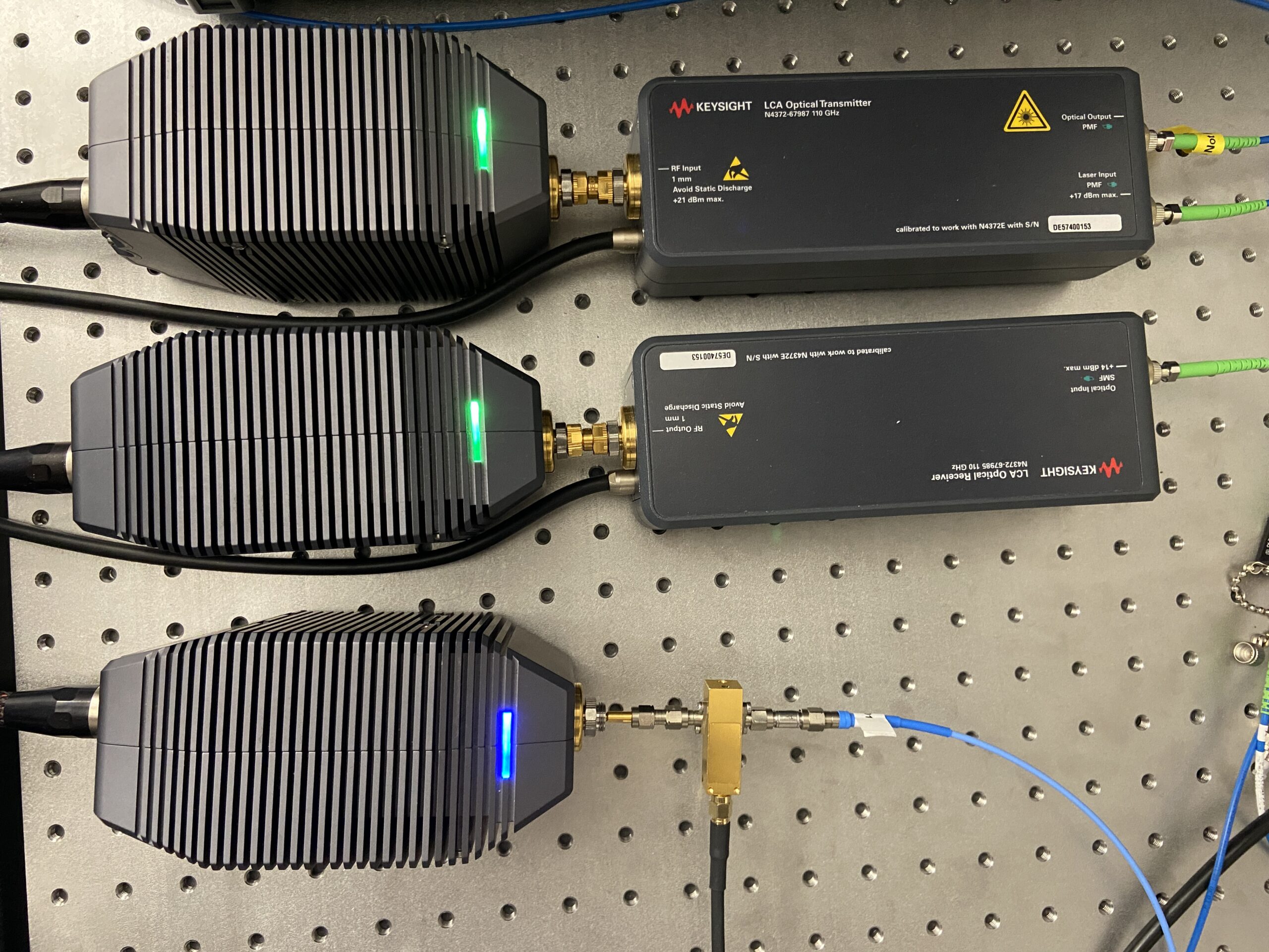
- Precision instrumentation: Built around the Keysight N4372E – a 110 GHz LCA with NIST-traceable calibration – ensuring high-precision, repeatable, and industry-aligned results.
Measurement capabilities
- EE / EO / OE / OO vector S-parameter measurements (S11, S21) from 10 MHz to 110 GHz
- Frequency-domain characterisation: 3 dB bandwidth, frequency response, flatness, and electrical/optical return loss
- Built-in optical source: dual fixed DFB lasers at 1310 nm (O-band) and 1550 nm (C-band) – the primary wavelengths for silicon photonic and InP device characterisation
- Extended wavelength coverage: 1260 – 1620 nm (O, E, S, C, and L bands) via external tuneable laser source, enabling wavelength-dependent frequency response measurements across the full telecom window
- Multiple measurement formats: log magnitude (dB), phase (°), group delay, linear amplitude, and complex (real + imaginary) – supporting comprehensive device modelling and system simulation
- NIST-traceable calibration for guaranteed, repeatable EO S-parameter accuracy
Custom test support
- Chip-level device configurations supported
- Non-standard wavelengths accommodated via external laser source integration
- Bespoke electro-optical probe and fibre configurations for non-standard chip formats
- Integration with customer-supplied equipment where required
Who this is for
Whether you are an industry partner developing commercial photonic components or an academic team pushing the boundaries of new device architectures, our facility provides the high-speed electro-optical test infrastructure you need to measure with confidence and move development forward.
- High-speed modulators (R&D) and pre-production qualification
- Photodetector and integrated receiver bandwidth verification
- Silicon photonic and InP transceiver characterisation
- PDK compact model parameter extraction and design kit validation