Introduction to Fabrication
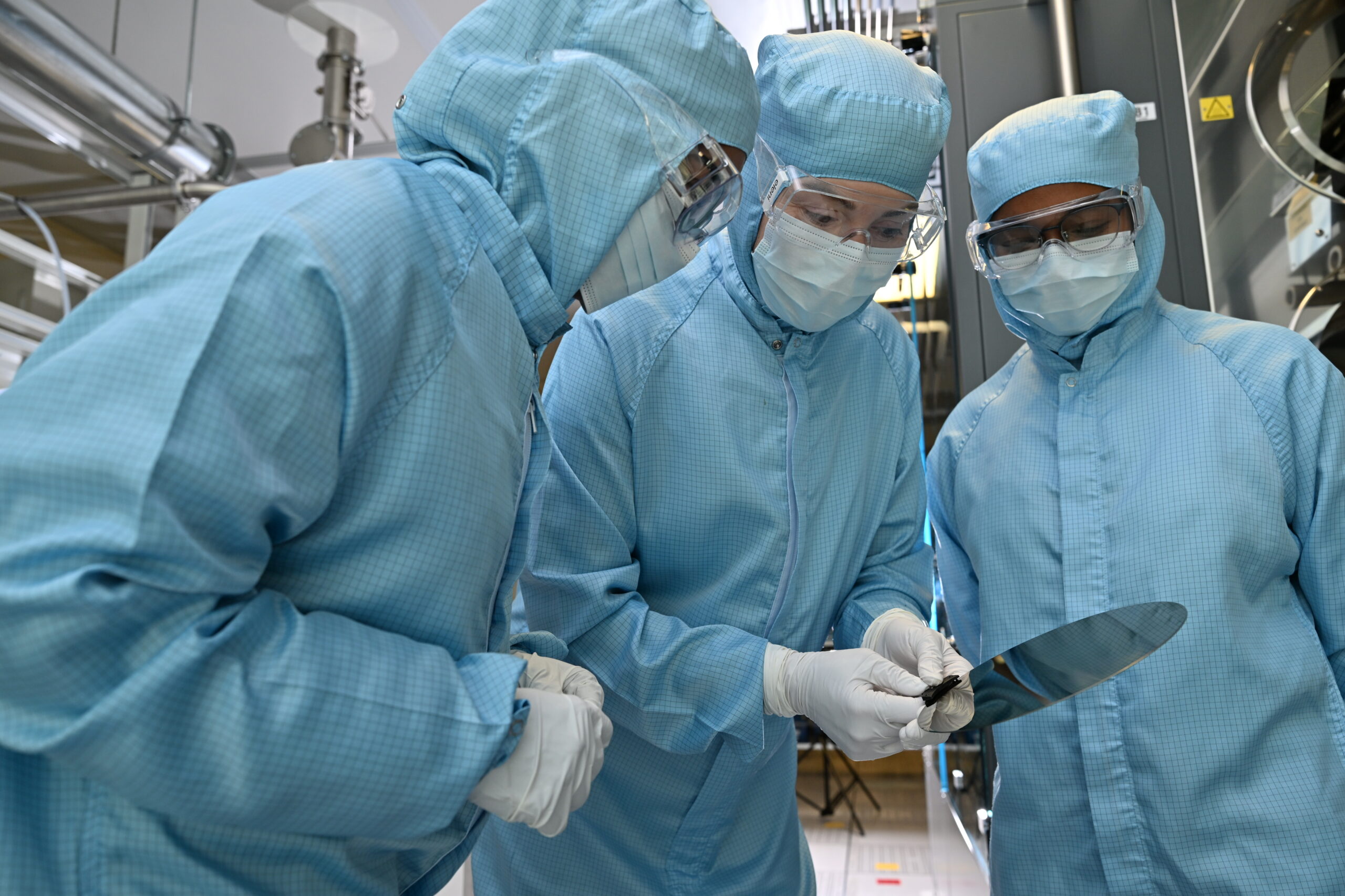
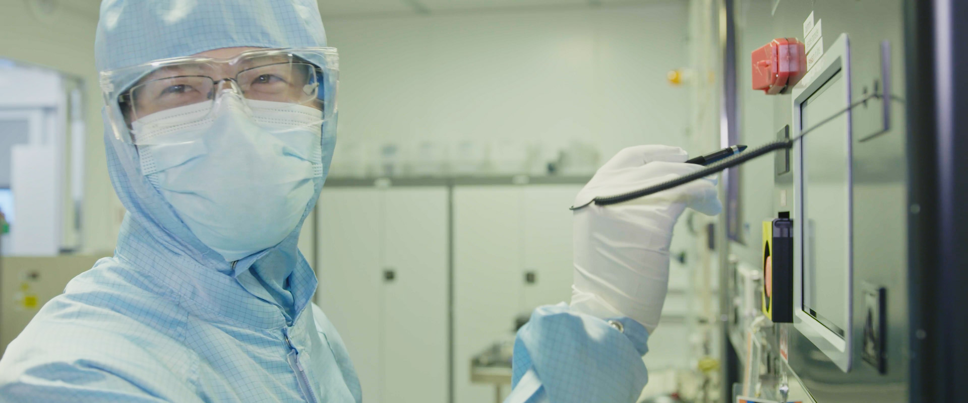
This two-day practical course provides a comprehensive introduction to the nanofabrication of silicon photonic devices. Delegates will gain hands-on experience with standard CMOS processing steps, key fabrication techniques and cleanroom protocols within the University of Southampton’s CORNERSTONE cleanroom facilities.
This practical two-day course provides hands-on training in the silicon photonics fabrication process, taking delegates through a complete fabrication sequence beginning with a silicon-on-insulator (SOI) wafer.
Through practical cleanroom sessions, delegates will gain experience in deep ultraviolet (DUV) lithography, silicon etching, cladding deposition, aluminium and titanium sputter deposition, wafer dicing and optical measurements. Supporting lectures provide the theoretical context behind the fabrication processes, alongside training in cleanroom health and safety and operational protocols.
What will you gain?
- An understanding of the full silicon photonics fabrication workflow and the processes involved in creating photonic devices.
- Practical experience of DUV lithography, including spin coating, photoresists and supporting metrology.
- An understanding of wet and dry etching processes, including the principles of ICP etching.
- Experience of cladding and thin-film deposition, including aluminium and titanium sputtering.
- An understanding of wafer dicing and the processes involved in chip separation.
- Experience of on-wafer and chip-level optical measurements, including alignment and fibre-to-waveguide coupling techniques.
- An understanding of cleanroom protocols, health and safety, contamination control and appropriate cleanroom procedures.
Pre-requisites:
The course assumes a basic familiarity with the process flow used in silicon photonics fabrication and a foundational understanding of optics and the relevant underlying physics. The course is designed to be self-contained, so previous cleanroom fabrication experience is not required.
Course Schedule
DAY 1
- Registration and course introduction
- Introductory lectures and tutorials
- Cleanroom health and safety briefing
- Cleanroom gowning demonstration
- Begin practical rotations across six fabrication and measurement station
DAY 2
Delegates continue rotating through the six practical stations:
- DUV lithography
- Etching
- Cladding deposition
- Titanium/aluminium sputtering
- Wafer dicing
- Optical measurements
Fees
- Standard Rate: £2000
Date: 23rd – 24th February 2027
Location: University of Southampton
Stay in touch
We’d love to send you our newsletter. You’ll be the first to hear about the latest MPW runs, training opportunities and news.
Join Mailing List