
Work Experience with CORNERSTONE: Exploring the World of Silicon Photonics
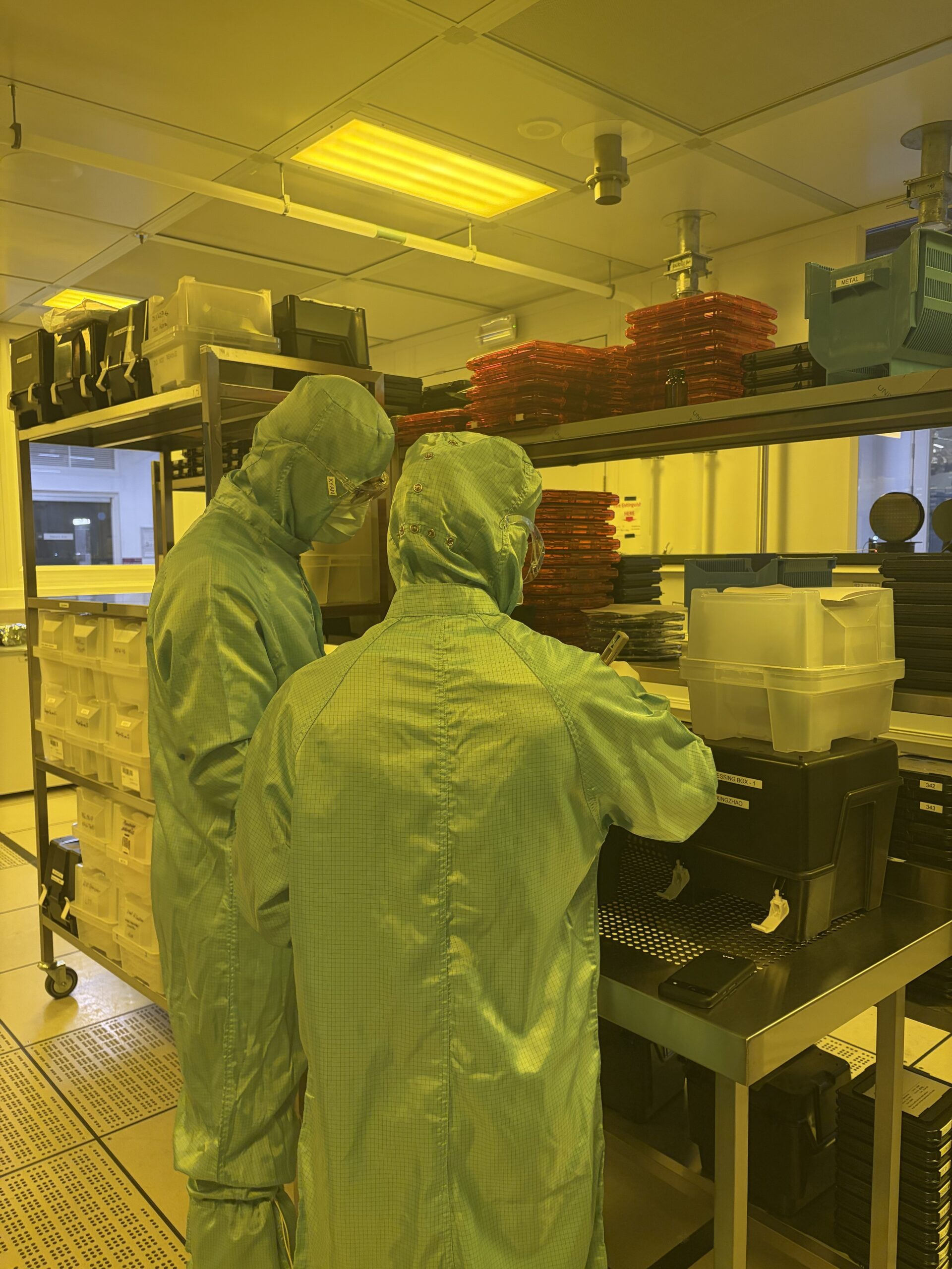
On 22–23 July, we were delighted to welcome two A-level students to Cornerstone as part of the LifeLab Work Experience Programme at the University of Southampton. This placement provided a unique opportunity to experience the cutting-edge research, engineering, and innovation behind silicon photonics technologies.
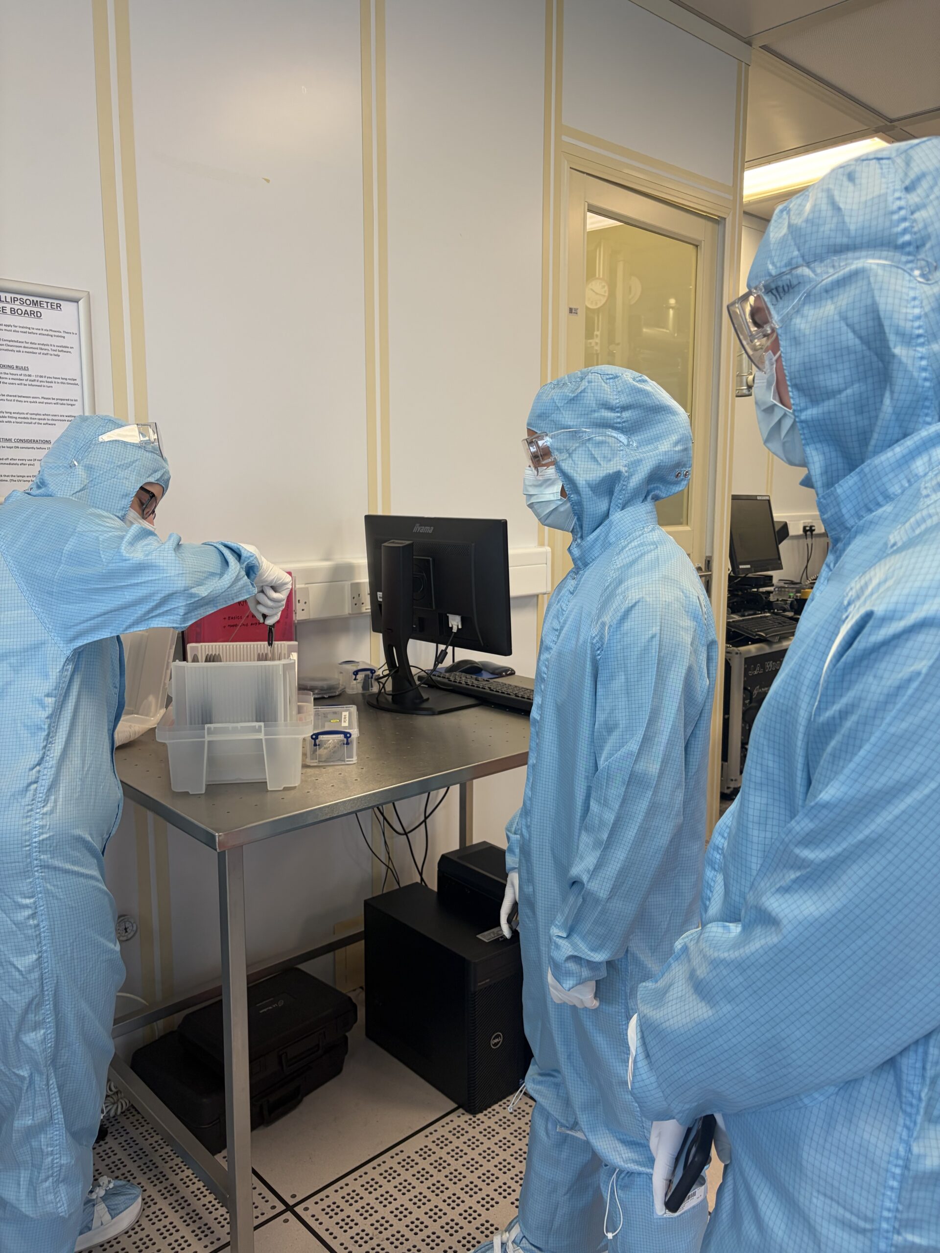
Throughout the two-day placement, they explored how photonic chips are designed, fabricated, and characterised, gaining insight into the highly precise processes involved in semiconductor manufacturing. They visited our advanced cleanroom facilities, learnt about fabrication techniques including photolithography, and engaged with our team of researchers to understand how silicon photonics is helping to address challenges in areas such as communications, healthcare, and future technologies.
A key part of the placement was discovering the importance of science communication. As part of their time with the team, they designed their own public engagement activity inspired by photolithography, translating complex research concepts into an accessible and engaging activity for wider audiences, specifically young people. They also reflected on their time with the team, sharing their thoughts and experiences in the testimonial below, written in their own words.
“Recently, we were lucky enough to undertake a work experience placement with Cornerstone. Over the course of two days, we gained an insight into the research and technology being developed by the team and how these discoveries could shape the future. Before starting the placement, neither of us had heard of silicon photonics, but we now have a much greater understanding of its potential and the ways it could transform different fields and people’s lives.
At the beginning of the placement, we were particularly interested in the potential medical applications of this technology. However, after speaking with the team and learning more about their work, we came to appreciate the much broader impact of silicon photonics.
One of the highlights of the experience was visiting the cleanrooms and seeing the precision involved in creating microchips. We had the opportunity to handle wafers, observe fabrication equipment in action, and use an ellipsometer, which helped us better understand the processes behind semiconductor manufacturing. We also enjoyed gowning up and learning about the importance of contamination control, and how even small particles can affect months of research and development.
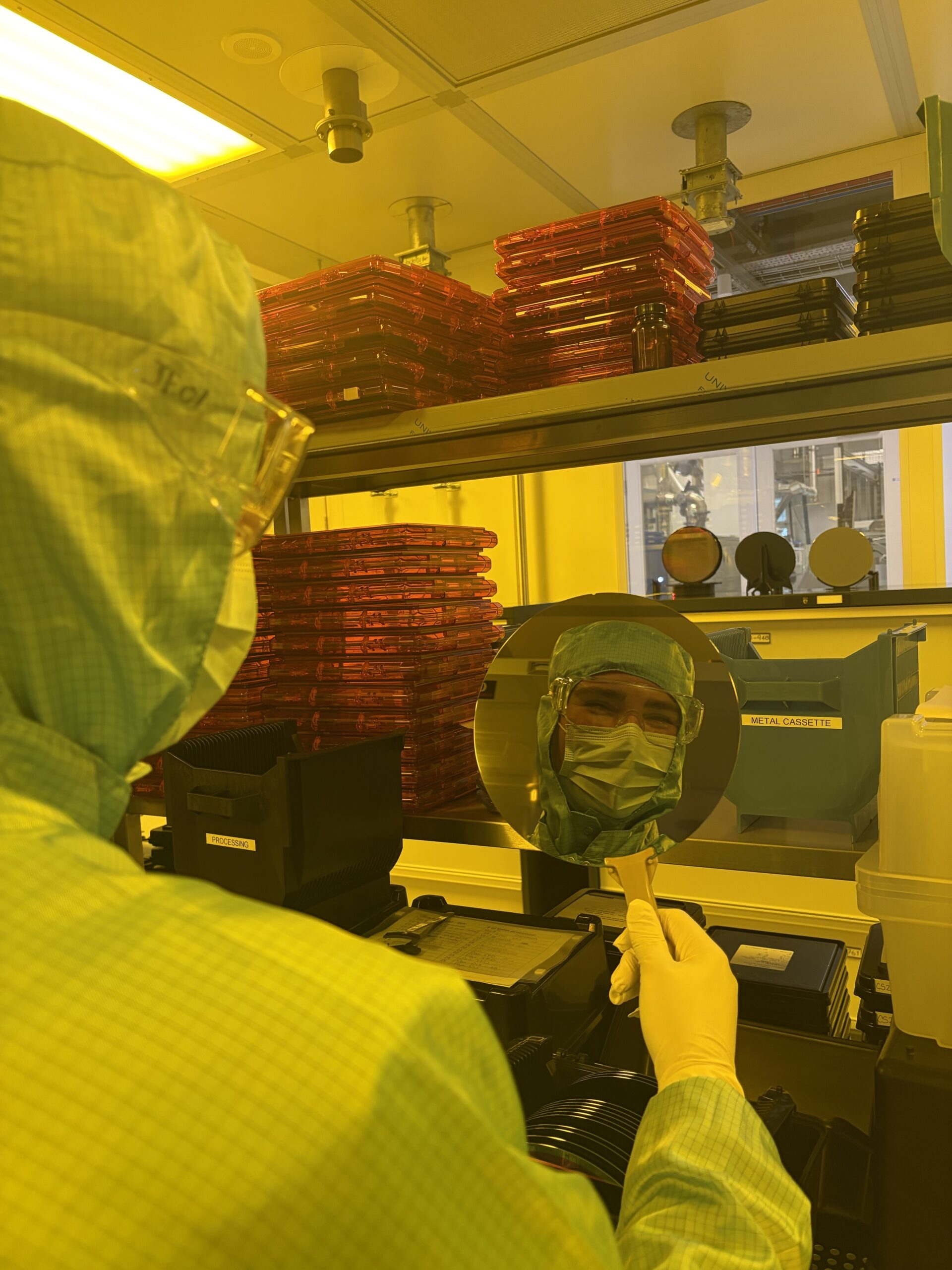
The placement gave us a greater appreciation of the innovation, skill, and collaboration behind silicon photonics. It was fascinating to see how fundamental physics can be translated into real-world technologies that could improve areas such as healthcare and the sustainability of data centres.
This was a valuable and inspiring experience, allowing us to see the people behind the research as well as the technology itself. We would highly recommend it to anyone interested in physics, engineering, and the practical applications of science.”